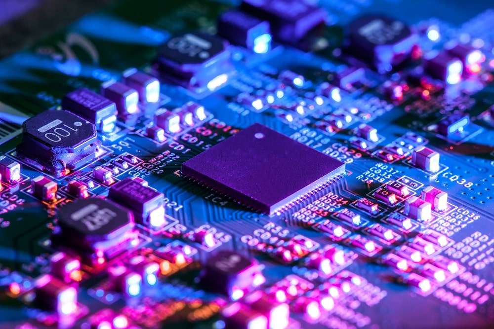
ACS Industrial has repaired thousands of circuit boards. But have you ever wondered how and why circuit boards are made? No matter how large or small, complex or simple, the basics of circuit board development are similar.
Here is the story of the development of a circuit board that was built for NASA. The space flight application for this particular circuit board is very specialized, but the process used to develop it is much like that in any other piece of industrial electronic equipment.
Most circuit board creation follows this basic process:
1. Decide – What do the electronics need to do?
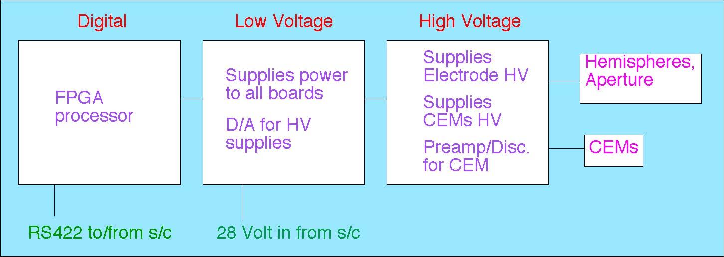
In this NASA board example, early in the development of the instrument, it was determined that the electronics could be divided into three categories: digital, low voltage, and high voltage based on tasks the electronics would do.
2. Obtain the components – How can we build the electronics with the components available now?
Electrical engineers are typically in charge of circuit board development. In this case, an electrical engineer worked to find currently available electrical components that could do the work needed for the instrument. While some circuit board requirements are simple, restrictions such as MIL-SPEC (certified to be rugged enough for U.S. military use), lightweight, low current, low-outgassing, etc. made the selection of components of this board more difficult. Eventually, the electronic components were decided on and samples were ordered for testing out in the lab on a ‘breadboard’. ‘Breadboards’ are simply boards that components can be arranged on without soldering. The circuits can be tested for function, and, if needed, one component can be easily replaced with another in an attempt to improve performance. They are called breadboards because, in the early days of radio, amateurs attached bare copper wires and components to a wooden board that was, or looked like, a kitchen breadboard.
3. Circuit Board Design Flow – How can we fit the electronics on the circuit board(s)?
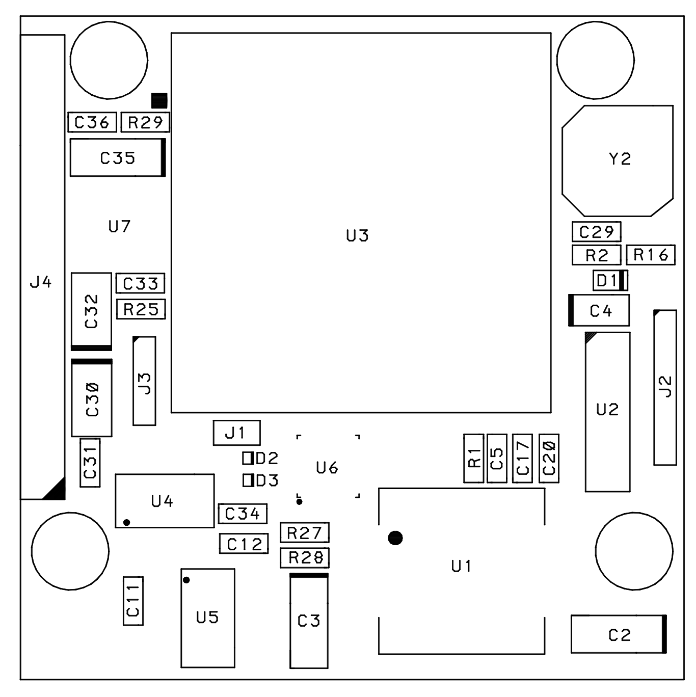
After the components were selected and the electronics were tested on the breadboard in the lab, we decided that a three-board arrangement would fit better in the small volume available. The entire instrument was then designed to contain three, three-inch square boards.
4. Finalizing – Firming up the board design
The arrangement of the components on the boards was optimized using software that simulated the function of the components. Simulating how components might interfere with each other, how the heat would be dissipated, and so on, helped us decide on the best location for each component on the board. Specialized computer files were then made of each board so we could have them manufactured.
5. Getting PCBs Made – Board manufacturing.
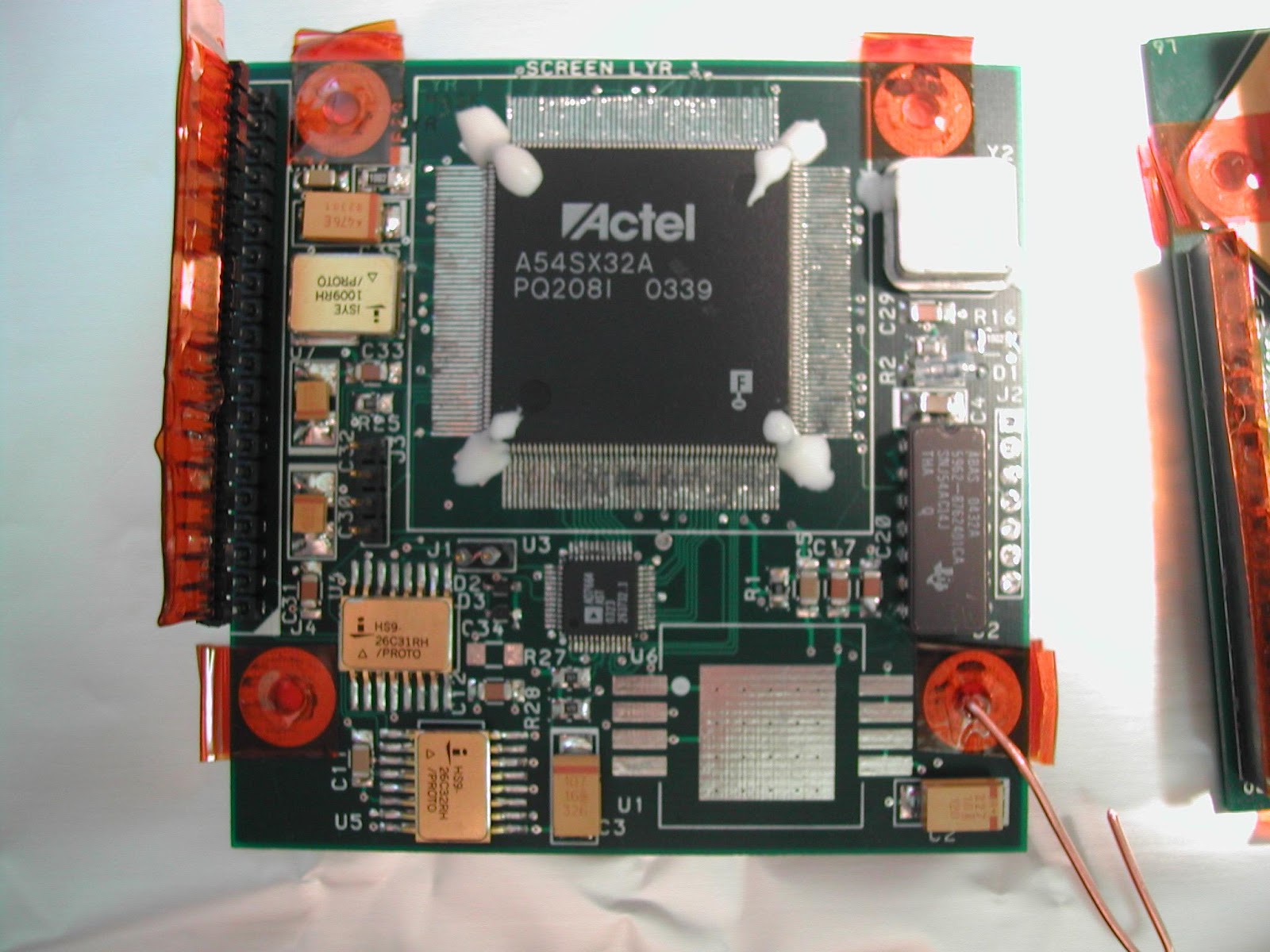
The boards were manufactured using ‘Gerber files’. A Gerber File is a type of computer file used throughout the electronics industry to describe the printed circuit board in great detail for its manufacture. The file contains all the information needed to produce the boards: precise locations for through holes, solder pads, conductive traces, etc. on each layer of the board. Various materials can be used for boards. A woven fiberglass cloth impregnated with an epoxy resin was chosen for this board due to its rigidity and low-outgassing properties. The board manufacturer made the boards by placing a protective mask on a copper-coated board then etching the board to create the copper traces, plating the board with solder, tin, or gold, laminating multiple boards together into a layered board, then drilling holes into the board where needed for mounting components or structural supports, etc. The completely finished boards were then tested for function and durability.
6. Testing the Boards
As you might expect, NASA flight requirement testing is very demanding. Not only were two versions of the boards required after testing began, but a component of a board failed during vibration testing and had to be replaced with a sturdier one, and epoxy staking and the conformal coating were required to assure the microprocessor chip wouldn’t shake off the board during launch into space.
Your circuit boards may not be launching into space, but they still went through all of these development stages and have specific performance requirements! Your board’s components and traces need to hold up, often in demanding environments with heavy vibration. Sometimes the harsh environment or simply aging components can cause your equipment to fail. The good news is that most industrial electronic equipment can be repaired!
This post touches on all that goes into the birth of a circuit board. So, the next time you send a circuit board to ACS because it has failed, you may look at your board a little differently. You can imagine all that went into building it, where it might have failed and how it can be repaired!
ACS guest writer, Dr. Luke Goembel, has published articles in Review of Scientific Instruments, Journal of Spacecraft and Rockets, IEEE Transactions on Plasma Science, Journal of Geophysical Research, American Bee Journal, The Woodwind Quarterly, and others.